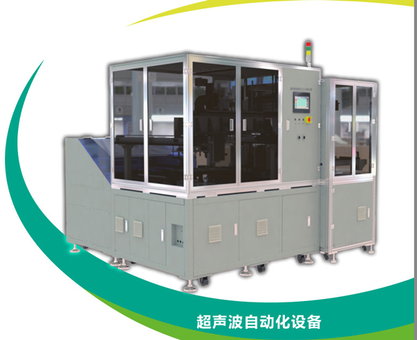
Scanning Acoustic Tomography (SAT) is a valuable tool in the semiconductor industry for non-destructive testing and evaluation of semiconductor materials and devices. This technology utilizes sound waves to create high-resolution images of internal structures, defects, and material properties, providing critical information for quality control, process optimization, and failure analysis.
1.Understanding Scanning Acoustic Tomography (SAT)
SAT works by transmitting ultrasonic pulses into the material being tested and measuring the time it takes for the echoes to return. This data is then used to construct a three-dimensional image of the internal structure, allowing analysts to visualize and assess the quality of the material.

2. Preparation and Setup
Before performing SAT, it is essential to prepare the semiconductor sample properly. This includes cleaning the surface to remove any contaminants that could interfere with the sound waves and ensuring the sample is positioned correctly for scanning.
3. Performing the Scan
During the scan, the sample is placed on a stage that can move in multiple directions, allowing the ultrasonic transducer to scan the entire surface. The transducer emits ultrasonic waves, which penetrate the material and are reflected back by internal structures and defects. The reflected waves are then detected by the transducer and used to create an image of the internal structure.
4. Image Reconstruction
Once the scan is complete, the data is processed using specialized software to reconstruct a detailed image of the internal structure. This image can reveal defects such as voids, cracks, and delaminations defects, as well as provide information about material properties such as density and elasticity.
5. Analysis and Interpretation
The final step in using SAT in the semiconductor industry is to analyze and interpret the images produced. This can involve identifying and quantifying defects, assessing material properties, and correlating the findings with other test results to gain a comprehensive understanding of the sample’s quality and characteristics.
In conclusion, Scanning Acoustic Tomography is a powerful tool for non-destructive testing in the semiconductor industry, providing valuable insights into the internal structure and properties of semiconductor materials and devices. By following proper procedures for sample preparation, scanning, and image analysis, SAT can help semiconductor manufacturers improve product quality, optimize manufacturing processes, and reduce the risk of defects and failures.
How to use a Scanning Acoustic Tomography in semiconductor industry ?
